Five industries which use printed circuit boards
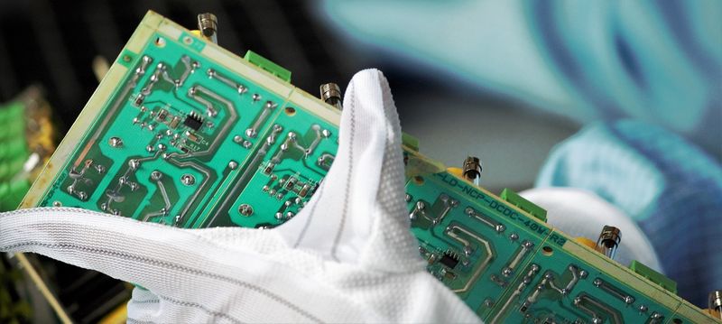
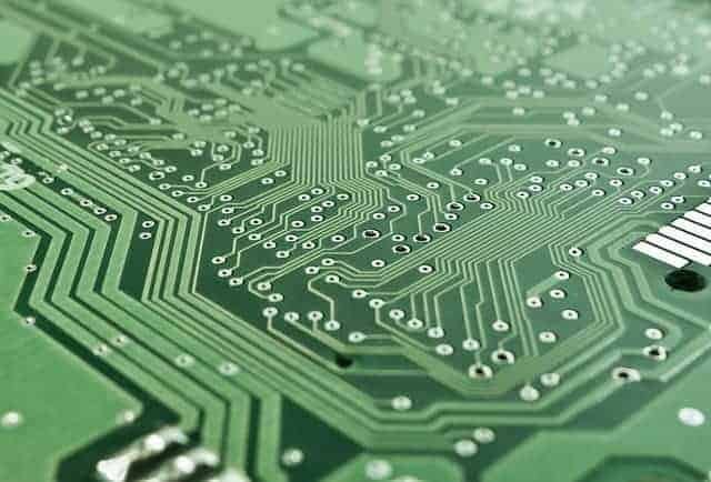
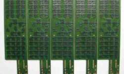
Printed circuit boards are the most essential components in all electronic appliances and products. Most of use these boards every day without even realizing what they are. If you ever open up your broken remote, you will see a circuit board which is infused with a lot of wires; it is called the printed circuit board. They are an integral part of electronic devices and are used in our everyday lives. They have many lines on them and continue to be infused in all electronic devices until this day. These boards are responsible for connecting the product to the wires via copper sheet. They are commonly used by the following industries: