
Electronics design is a specific niche that involves lots of building steps and expertise. Each electronic device has overcome many manufacturing and refining cycles until it is safe to use. Blends within the environment have necessary and useful features and are much supported. Everything starts from the need for functions electronics can provide. A simple LED lamp is a complicated product that needs to last, operate within specifications, and overcome certifications to be safe to use as a home appliance. It is hardly achievable by a single person.

The core of almost every electronic device is its working circuit laid on PCB. Let’s go through PCB manufacturing processes to see what steps are usually involved until design reaches production.
PCB design cycles
It all starts with the specification. Depending on the needs and functionality, specifications are defined – what circuit will do, what the limitations are, and how it will be controlled. According to specifications, the initial circuit design is created. Then follows the PCB layout. If there are programmable devices used in parallel to circuit design, program design can be prepared. Until there, everything can be done virtually using computer software.
The following process involves physical manufacturing. First of all, a PCB prototype is made in a fab house, such as PCBWay. It produces a PCB according to the PCB layout. Depending on the design, a PCB can be any type such as standard multilayer FR-4, Aluminum or Copper base, flexible, rigid-flex, and of other advanced material as HDI/Rogers/High-Tg.
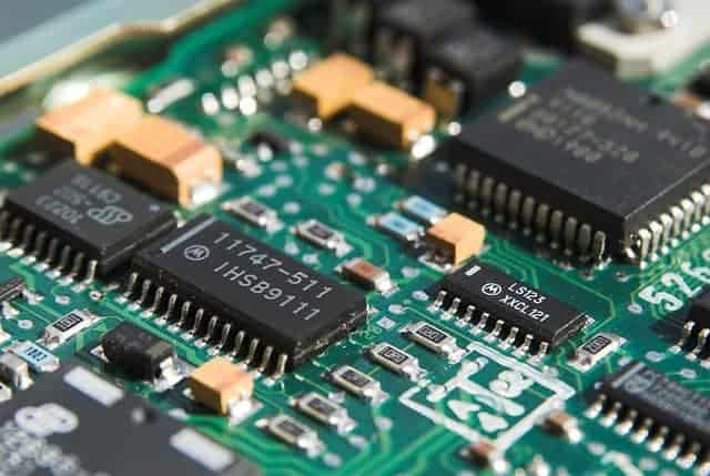
After the PCB prototype, a PCB assembly is performed. During the assembly process, through-hole, SMT, and more advanced such as BGA or fine-pitch electronics parts are placed on the PCB and soldered. PCB Assembly process goes through testing procedures such as visual inspection, x-ray, AOI testing, in-circuit testing, and functional testing. Optionally products can be ISO9001 certified.
After the initial manufacturing cycle, the device can go straight to production or have revisions when errors are fixed, functionality expanded and design changed. There can be as many revision cycles as needed. Usually, complex circuits have many reviews until the design satisfies the required functionality.
PCBWay can cover all PCB manufacturing processes
After we roughly covered PCB design and manufacturing processes, we can look at what procedures may be eased by PCB fab such as PCBWay.
PCB prototyping
The primary and core function of the PCB fab is to manufacture PCB prototypes. They have developed a convenient and functional PCB prototyping quote form, which expands for selecting tons of parameters according to your design.
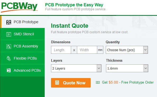
It is hard to cover all the possible options. We can mention several that may be important initially. The basic settings are size and quantity. For instance, 10 pcs of 2-layer 50x100mm are as cheap as $5 without shipping cost. And manufacturing is finished within 24 hours. You can tweak many PCB parameters such as board thickness, solder mask, silkscreen colors, surface finishing, copper track thickness, way of panelization, and the number of layers with different processing of vias. If you select different than the default option, you should already know what you are doing and be prepared to pay more as these involve nonstandard operations that stand out from the normal routine.
Even more, if you choose different base material than standard FR-4, you are opted in to even more options. Let’s take a glance at what are other prototyping materials available.
- Advanced Rigid PCB technologies. These include high tech and quality boards based on /HDI/Rogers/High-Tg technologies usually purposed for high-frequency electronics, automotive, and other particular purposes. Choosing those boards to require a different level of expertise in designing PCBs.
- Aluminum PCBs. It is possible to select two types of aluminum PCBs – central and base core where choice depends on desired power dissipation properties and mechanical stability.
- Copper PCBs. There is an ability to substitute aluminum with copper for better thermal performance and other specific properties but at a higher cost.
- Flexible PCB. These types of PCBs are used in nonstandard type portable devices or miniature electronics. They allow squeezing complex circuits in tight spaces. Typical electronic devices with flexible PCBs are cameras and smartphones.
- Rigid-flex PCB. This technology joins flexible and rigid PCBs into a single unit without connections between them. In such a way, manufacturing becomes easier and cheaper while having the benefits of both technologies.
PCB assembly
We have already covered some key points of PCB assembly service capabilities and benefits in the previous post (The top benefits of low-cost PCB assembly service). Anyway, PCB assembly takes the PCB prototype and populates it with electronics components included in the circuit. This way, you don’t need to make stencils, prepare equipment, place and soldering components, and ensure quality. All those steps can be performed by PCB fab.
PCB prototype and assembly tandem take your design files and convert them into the real physical working device. Ideally, all this can be accomplished within a couple of days – 1 day for prototyping and another for assembly. The basic board can cost $5 for prototyping and $30 PCB assembly (without parts included).
PCB design service
There is still an electronics design that needs to be taken care of. There is a standard practice that you provide design files to the manufacturer for prototyping and assembly. But what if the design process could also be assigned to fab. All it would be best if you delivered rough specs, and that’s it. This is where PCB design services come in.

The PCBWay are incredibly flexible with their services:
- Electronic design, including technical project management. They are capable of using the most popular EDA software for designing, managing, and documenting projects. Along with third party product design companies, they can provide a wide range of high-quality services from start to finish.
- Financial management of the project. PCBWay can keep track of budgets and costs remotely. All the ongoing cash flow is managed effectively on site.
- Software and Firmware programming, implementation, and IT management. They can offer a wide range of software and firmware development options. According to your specs or general concepts, services may include programming embedded devices, app development for platforms such as Windows, Linux, Mac OS, or Android applications.
- Mechanical design of the project, including 3D modeling and realization. Suppose your product needs an enclosure, shape, and form produced by mold injection or even 3D milled or printed.
- Documentation from start to finish. The least favorite part of the design – The project’s documentation and the final device can be taken care of with a professional attitude and requirements.
As we see, the PCB way can take care of all product development steps: design, prototype, and assembly. Design service may require the most significant investment. Still, in the long run, it may save lots of time and money as a process involves highly experienced professionals leading to fewer errors and delays. Check out the other capabilities of the PCBWay fab house.