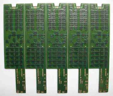
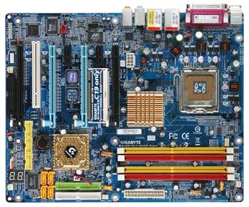
The term circuit technology usually refers to the various techniques used in the manufacture of electrical circuits. A large number of devices that are used today make use of printed circuit boards (PCBs). These devices provide mechanical support for the various components present within the given device and the components’ electrical connections.
The electrical connections present on the PCB are made out of copper sheets laminated on a non-conducting material. Initially, a large copper sheet is laminated on the board, and then the sections that are not required are removed. Various techniques are used for the removal of unwanted copper. Some of them are:
- Silk Screen Printing: In this technique, an etching-resistant ink is applied to those required areas, and the remaining part is etched off.
- Photoengraving: Here, a photomask of the circuit required is prepared using the desired software, and then it is applied to the blank PCB. After this, the portions that are not required are etched off.
- PCB Milling: In this technique, a mechanical milling system that can work on 2 or 3 dimensions is used to remove the copper. The milling system is controlled by software.
In some other techniques, only the required copper is added to the board.
After this process, holes are drilled on the PCB as required. Again this process is controlled by computers to attain the necessary accuracy. In some cases, printed circuits are present on both sides of the board. The two sides of the boards are interconnected by hale with copper plating on their surface.
The boards’ surfaces where the components are to be mounted are coated with specialized materials as copper tends to oxidize at a quick rate.
After the completion of the etching process, the boards are coated with a layer of tin. This helps in maintaining their solderability even after storing them for a few months. The information about the various components present in a PCB can be printed on its surface using screen printing. New digital techniques have been developed for screen printing that can accurately print bar codes on the surface.

Before the connections are mounted on the board, every connection present on the board is tested. Various techniques may be used for the same. Specialized tests such as the “Bed of Needles” test are used in the case of PCBs that are mass-produced.

After the testing process is completed, the various components are mounted on the PCB. By using some techniques, the pins of the devices are inserted into the holes present on the PCB. This completes the manufacturing process of the PCB then, it needs a safety certification and then, it can be introduced into the market.
There are many examples of PCBs. For example, the motherboard present on the computer, the RAM, etc., is PCB. They are also used in various other devices such as remote controls, calculators, etc.


PRODUCTS: “We customize it; anyway you requests:”
Medical Device electronics, Single and Multichannel Inputs, A/D 24/32 bits, 4 to 32 Channels; Supporting Open Hardware and Open software
CNC System; Laser Cutting, CNC Milling , CNC Punch; provide software and/or motor control board for AC/DC Servo or Stepper!
ELECTRONICS OPEN-FRAME BOARDS:
FPGA CPU, with USB, Ethernet, Wireless
A/D 24/32 bits, 4 to 32 Channels
CPLD with FIFO and USB
Micro Controller with USB and Ethernet
CNC FPGA Board + Software “Mill, Cut, Punch”