Today most of all embedded systems consist of two-part circuitry – digital and analog. The Digital part is usually the controller, its timing circuit, and other input-output devices. Frequently there is an analog part on the same board like ADC, OP amplifiers, sensors, and other analog circuitry. Such designs are called mixed-signal designs. Where digital and analog parts meet – the grounding problems start. The fact is that each conductor has its own impedance, so any current flowing results in voltage drops. Ground wires and planes aren’t exceptions. Digital and analog grounds can generate significant electromagnetic radiation that adds noises to signals we need. So the overall system quality drops because o poor design.
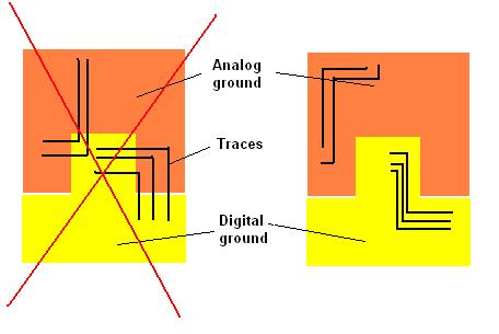
In a good design, the analog ground plane and the digital ground plane should be separated. With multilayer PCB, this can be done very easily. Another issue is that digital signal traces shouldn’t cross analog ground, and analog signal wires shouldn’t cross the digital ground plane area. Of course, try to avoid aligning digital and analog wires as they can catch each other radiated noise.
How to deal with these problems. Well, the first thing is to recognize problematic areas correctly. Then you will be able to implement the right design. The correct implementation is all about correct part placing and correct wiring.
If there are more than one analog parts on the board, then each of them should be separated so that even different analog parts don’t overlap.
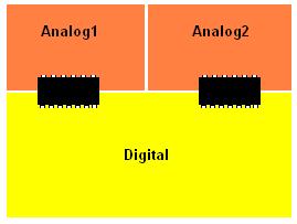
According to this example, it is important to say that each good IC manufacturer is trying to separate analog pins from digital pins in a package. For instance, let’s take Atmega8. See how nicely analog part is separated from digital part:
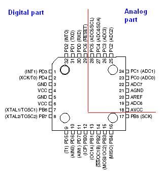
So that easier could be digital and analog part separated on PCB.
One more actual problem I want to mention here is ground loops. Ground loops exist when electrical devices are connected to the ground in more than one way. Simply speaking, if devices are connected to more ground pints than on, then a ground loop exists. Ground loops can generate significant noise, especially in audio and video equipment. The following example represents wrong ground implementation as there is an obvious ground loop:
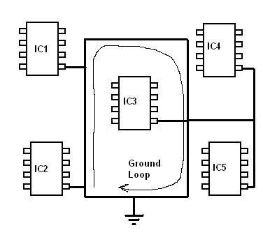
For example, above the ground has one loop, and the bigger loop(, the longer wire), the more noise it will pick up. So the circulating current will generate more noise radiation. There only one suggestion is to use common ground point or so-called tree-like grounding:
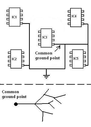
Usually, ground loops are a post-factum problem – when you realize that the system is generating too much noise. The only solution can be to cut a ground loop path, hoping that this helps a bit.
So by concluding we can generate some general rules, how to correct grounding should be done:
- The first rule is – Try to separate analog and digital ground planes. This can be easily done in two and more layer PCB’s. With one layer PCB, there are many more limitations to do this, but you can again follow the idea and try to separate the analog part from digital.
- The second rule – Try not to cross analog ground with digital signal wires and avoid crossing digital ground with analog signal traces. Ideally speaking analog part of PCB should be totally isolated from the digital part speaking in terms of placing.
- The third rule – if it’s possible, try to keep ground planes as solid as possible. If the board is double or more layered, then one side of the board should be ground polygon. Remember, thicker wire is less impedance have it means less radiation because of voltage drops.
- The fourth rule – try not to align analog traces and digital that they could catch each other generated noise radiation.
- The fifth rule – avoid ground loops. Use Common ground connection or tree-like grounding structure.


I want to make a reference to the information posted here. Who should I quote ?
Very useful, thanks