
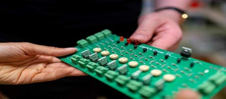
Printed Circuit boards (PCBs) are an essential part of an electronic device. PCBs’ function is to supply connection and wiring mechanisms for different components of a motherboard or an electronic device. In the past, PCBs were used in devices that limited functionality; therefore, it was easy to manufacture them. As a result of innovations, modern electronic gadgets are built to perform multi-tasking and require PCBs that are compatible to perform more complicated functions.
In this article, we will discuss the multilayer printed circuit board (PCB) and the benefits of using them in modern electronic gadgets along with their use in the equipment of different industries.
The simpler electronic gadgets with limited functions are composed of single or double-layered PCBs. Still, for more sophisticated electronic gadgets like motherboards of modern tablets or cell phones, multiple layer PCBs are needed. Multilayer PCBs are only capable of fulfilling the requirements of these modern and sophisticated electronic gadgets.
Defining Multilayer PCBs
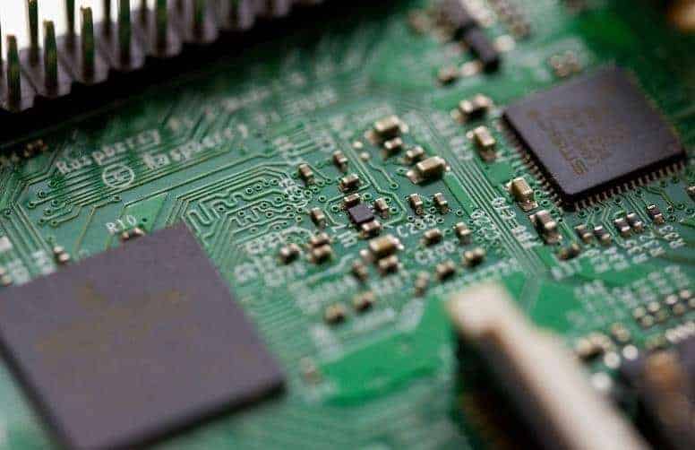
The multiple-layer PCBs are composed of three or more conductive copper layers. The copper layers appear as layers of the two-sided circuit board. These layers are either etched boards or trace layers. Today the multiple layer PCBs are much in demand to be used in modern electronic devices. Their ability to perform numerous tasks in a lesser amount of time and their small size has enhanced their need for modern electronic devices.
The layers of these PCBs are coated together through the lamination process; Extreme pressure and temperature are provided to the inner layer for lamination. After the lamination, the PCB is cured at extreme heat, after which the pressure is gradually released. Once the layers are laminated together, the PCBs can cool down by reducing the temperature. The layers face the two sides of the PCBs so that they connect to the environment.
From four layers up to twelve layers, the PCBs are being manufactured in varied sizes and thicknesses to meet the demand of electronic gadgets in which they are to be used. The layers of PCBs are mostly produced in an even number of layers so that they are more connectivity options and are cost-efficient.
Rewards of using multiple layer PCBs
The multiple layers PCBs have many rewards which single- or double-layer PCBs did not have. Continue reading to know more about them.
They are smaller in size
The multiple-layer PCBs have a layered design that makes them ideal for devices with smaller motherboards. As the technology moves towards smaller yet more powerful full gadgets like smartphones, tablets, and laptops, the use of multiple layers PCBs is continuously increasing due to their small size and efficient performance.
They are light in weight
As the size of the PCBs is smaller, they have less weight too. Earlier multiple connectors were used in the motherboards to connect single- or double-layer PCBs, which increased motherboards’ weight. During the evolution of multilayer PCBs, manufacturers were able to avoid those multiple connectors; thus, the motherboard’s weight has decreased too. The lightweight motherboards are ideal for portable devices.
They have better performance
There is much amount of work and planning that is done while manufacturing the multiple layer PCBs; therefore, they are result-oriented and better in performance as compared to single- or double-layer PCBs.
They are more durable
The multiple-layer PCBs are designed and produced in such a way that they are capable of handling elevated temperatures. As they handle more amount of heat, their durability is better than single- or double-layer PCBs
They are faster & powerful
As multiple layers are being laminated in a single PCB, it has small quarters in multiple layer PCB. A higher number of layers are being laminated in a single PCBs; therefore, it has small quarters. As the area of these quarters is lesser, they have the ability to supply powerful electrical connections. Moreover, they have more exceptional ability and speed due to their compact size and efficient electrical connections.
They have single connection Point
The multiple layer PCBs are designed to run as a single unit; therefore, they have a single connection point in the motherboard. As they have a single connection point, it requires lesser space in the board. This characteristic of multiple-layer PCBs has enabled the manufacturers to design the board more compactly.
Usage of Multi-layer PCB’s
As discussed above, there are many advantages of Multi-layer PCBs. We have already been talking about their use on the boards of modern electronic gadgets, so that you might have a question about their usage in other industries?
In the upcoming text, we are going to discuss different industries in which multiplayer PCBs are used.
Electronic devices
The electronic devices that we use in our daily lives run so efficiently because of multiple layer PCBs in them. From microwave ovens to smartphones, all electronic gadgets have numerous layer PCBs. The trends of consumers have changed with time, so have the hardware of consumer electronics. Every one of us wants to be surrounded by smart devices. This has compelled the manufacturers to include multilayer PCBs in the electronic devices as they are capable of multi-tasking and are compact.
Communication Devices
The multilayer PCBs are also used in the devices which are used for communication. They are used in these devices because they are efficient in performance and are long-lasting. The multilayer PCBs are used in mobile applications such as GPS, signal transmission, and satellite services, including outdoor towers. As these PCBs are used in devices exposed to nature, durability is needed to make them long run.
Health care devices

Multiple layer PCBs are also used in health care devices. The multilayer PCBs are used in health care devices because they are small, are efficient in performance, and are lightweight. For example, they are being used X-ray machines, heart monitors, and CT scan machines.
The multiple layer PCBs are also used in the following industries
- Aerospace
- Automobile industry
- Defence industry.