When building an AVR DDS2 signal generator, there were many discussions about signal conditioning in the analog part of the device. The first argument was that LM358 wasn’t the best choice for this purpose. Another one pointed to the sine wave that wasn’t smooth enough.
As you can see, there are some dents on it. Other waveforms also are distorted, especially when higher voltages are selected. This asks for a better analog part. Some people suggested replacing LM358 with OPA2134, but it seems to be quite an expensive choice. In my opinion, low noise, a general-purpose op-amp can be great too. I’m going to give a try to Texas Instruments TL074 low noise op-amp. It is low power, high slew rate (13V/us) IC – almost five times faster than LM358 and for the same reasonable price.

If we look at the DDS2 signal generator offset and gain control circuit, we can see a problem with it. We regulate offset before amplitude control – usually, offset should be adjusted after amplifying the signal. And the third problem is that offset can be handled in the small interval – in the 5V range, while we could do this in the -12V … +12V range. Let us redesign the analog part so it would give a better result.
Zeroing offset voltage
First of all, offset control, we can slightly modify the first stage so that the signal’s offset voltage would be set to 0. For instance, if we generate sine-wave on DAC, we get a maximum of 2.5V amplitude signal with a 2.5V DC offset. Instead of using POT1, we can calculate the resistor divider so that we get a 0V offset on the output. We assume that all signals coming out of the microcontroller have offset 2.5V (when VCC=5V), then we can model the following circuit:
Calculating is easy:
We know that the source voltage is Vs=2.5V. The output voltage is Vo=0V. We need a gain of 1 (-1 for inverting amp). So at inverting op-amp input, we get voltage:
From from operational amp analysis we know that V- = V+ and currents to both inputs are equal to zero (I- = I+ = 0A). Then We must get 1.25V at V3. so we need to select a voltage divider to scale voltage from 5V to 1.25. To do so, we chose one fixed resistor value R3 to be 100kOhms, and then we calculate R4:
evaluate R4:
We can get 33.33kΩ by connecting two resistors in series: 33kΩ + 330Ω that will give the resulting voltage close enough to 0V.
Optional filter stage
In the next step of the analog part, we are going to add a filter. Since the DDS signal generator is capable of outputting various types of signals, we don’t want it to be hardwired. For instance, if we generate a sine wave, then we could use a filter to make it more smooth while on a square wave it would have a negative effect by rounding the shape. For this, we can add a bypass switch that would allow to insert or bypass filter on demand. What filter are we going to use for this purpose? Since we have plenty of op-amps on TL074, we can make an active filter.
I find Butterworth’s (Sallen – Key) low pass filter quite handy since it gives the band’s flattest response. Let’s select parameters for this filter. DDS generator, in our case, isn’t going to exceed 100kHz frequency. Also, we want attenuation in this up to roll-off frequency near 0dB. So let us increase the roll-off frequency up to 200kHz. This value we are going to use while calculating.
Resistor and capacitor values of the filter can be determined with these simple rules:
R1 = R2, C1 = 2·C2
If we select R2 = R1 = 33k (have plenty of these)
then we can calculate C2 as follows:
so standard value of C1 = 33pF.
You can check calculations online here.
DDS Signal amplitude gain control
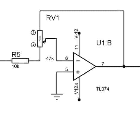
After we have adjusted signal offset voltage filtered it (or not), the next part will adjust amplitude. We need to adjust the signal amplitude from 0 to 12V. For this purpose, we are going to use an inverting amplifier with an adjustable potentiometer gain. We need to calculate proper resistor values to get excellent gain control over all potentiometer turn. Say we are going to use a 47k potentiometer. Let us calculate the input resistor value.
Another known condition is that the input voltage from the previous stage is 2.5V. Say we want to get 12V amplitude on the output we need gain: 12/2.5 = 4.8. If we turn the potentiometer to the max left, we get:
R1=47k/4.8=9.79k~10k. To get 0V amplitude, we need to turn the potentiometer to the right, so the gain ratio gets close to 0.
Signal offset regulation
And the last stage of the analog part is signal offset regulation. We want to regulate offset in the range of -12V to 12V. The easiest way to do so is to add an offset voltage to signal voltage.
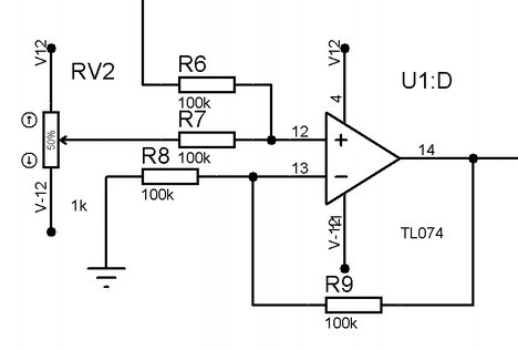
Since we already have two inverting cascades, we don’t want the last one to be inverted that would lead to an inverted signal on the output. So we are going to implement non-inverting summing:
Let us see how to calculate resistor values. R6 and R7 we select to be 100k resistors as they aren’t critical while in the recommended range of 1k to 1M. The more interesting part is the gain. Let us see how non-inverting summing amplifier output voltage looks like:
What we see here is a voltage added and multiplied by the gain. Since our R7 and R8 are equal to 100k, we get that only half of these voltages are added. So we need to adjust amplifier gain to 2 to operate with total values. So we need:
After solving we get that both resistors have to be equal. To keep resistor values less scattered we also chose those to be 100k.
Putting it all together
Now we have all blocks ready and can connect them into a single circuit:
Here we have linked all four modeled parts: offset adjust, low pass filter, amplitude control, offset control. TL074 chip comes with four operational amplifiers built-in to get away with a single chip and this functionality. If you are interested in simulating, here is the LTspiece simulation file. TL074 was replaced with a similar TL1359 op-amp in the simulator, so actual results shouldn’t differ much.
And corresponding signals on various nodes:
As you can see in the first stage, we have a sine signal with minor distortion added, and its offset is 2.5V. After offset adjusts signal still is distorted, but it crosses 0V now. After filtering, we see no more distortion – only smooth sine. Then next stage adjusts signal voltage gain, and on output, we get a signal with a selected offset somewhere at -5V. Results look promising, so the next step will be to put everything into a working project. Comments and suggestions are welcome.


Awesome!
I considered building the v2 version of this project, but now I’ll wait for the v3.
How about digital control for analog stage? We could add another cheap micro. This additional microcontroller could control lcd/keypad and reset DDS micro to change what it generates. It could also provide interface to a computer for automated tests.
I had some thoughts about controlling offset and voltage by using digital potentiometer. Using standard 256 step digital pots don’t allow fine tuning due to significantly large voltage steps. Another problem is additional board space. Probably intuitive potentiometer is good choice for now.
The idea of using additional microcontroller sounds great – especially when performance and flexibility is needed. But again – simplicity will be lost.
hi, i won`t build V2.0 but is there some .brd .sch for
V3.0?
Please answer
Greetings
Dirk
What about to create a function that we can design inside the chip the wave that we desire?
Perhaps read a potentiometer when we press a button?
Practically there is no need for potentiometer. All can be done with same menu buttons. Wave table consist of 256 8-bit values so every sample could be managed one by one selecting its value and storing it. No need for additional pot. Good suggestion.
I’ll second Joe’s opinion. We already have two great simple designs from you (I’m using v2 with great success). For v3 you should pursue performance and flexibility.
For those who need signal generator now, just build DDS2 generator schematic with planed DDS3 generators analog part, and it already will be much better. And for those, who wants some arbitrary waveform generator capability, just buy Rigol DG1022, it could be find for 400$ shipped. I bought one and I am realy happy with it, but I still use DDS2 for tasks where I need to generate more than two different signals, but now I plan to upgrade just analog part of it.
With DDS2 this analog part should work fine.
Can anyone comment on:
1. variable gain (pot in feedback loop). I guess it varyies freequency response of opamp and some opamps may start to oscillate on gains 20khz). Does anybody build analog part of Ver3 and can verify this?
4. Do we need to set output impedance to some value (say 600om) putting isolating resistor in series on output and terminate with same value close to oscilloscope input?
5. Also datasheet figures measured on 2k load. Do we need to provide some load after each opamp section?
<<<>
2. I think schematic also misses decoupling 0.1uF caps close to each opamp supply pin to GND, without this it should oscillate.
3. Also not sure regarding 100k resistor values. It should add noise and bouncing/ringing/overshooting problem on fast signal edges (e.g. rise/fall of sqare wave >20khz). Does anybody build analog part of Ver3 and can verify this?
Hi Ffa, there are definitely few problems with analog part. You can see few initial tests here: https://scienceprog.com/avr-dds3-first-tests/
It overshoots and rings on sharp edges. I am not that good at analog electronics so suggestions for improvements are welcome.