
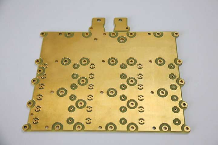
Heavy copper PCB, also known as thick copper PCB, is a printed circuit board with 3 ounces (oz) of copper or more on the internal and external layers. Moreover, a heavy copper PCB is a circuit board having a copper thickness of greater than 4 ounces per square foot (ft2).
What is the thickness of copper on a PCB?
The 1 oz completed copper weight selection is also the usual beginning copper weight for external layers on PCBs. Standard internal layer copper thickness for “standard construction product for 1 oz and 2 oz finished copper weight options is 1 oz copper (35m thick or 1.4 mils).
What is PCB copper weight?
First of all, in a printed circuit board, copper weight or copper thickness refers to the thickness of 1 ounce of copper rolled out over a 1 square foot area. A PCB with a copper weight of 1 ounce, for example, will have a copper layer that is 1.4 mils thick.
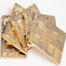
PCBs made of thick copper are widely utilized in power electrical devices and power supply systems. This unique sort of heavy copper PCB has a completed copper weight of more than 4oz (140m), compared to the 1oz (35m) or 2oz (0m) copper weight commonly found in those with a typical PCB copper thickness. It is an emerging trend in the PCB business.
What is the benefit of copper thickness?
The increased copper PCB thickness allows the board to carry more current. As a result, it achieves good temperature dispersion and allows complications in switches to implement in a small space. Moreover, increased mechanical strength at connecting locations is another benefit.
The construction of a heavy copper PCB provides a board with profits such as:
- Firstly, increased thermal endurance, increased current carrying capacity, and increased mechanical strength at connector locations and PTH holes.
- Secondly, exotic materials can be used to their maximum capability (high temperature) without causing circuit failure.
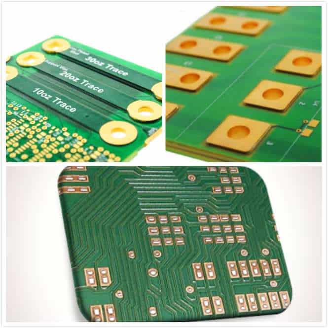
- Thirdly, multiple copper weights on the same circuitry layer resulted in a smaller product (see Figure 1).
- Fourthly, heavy copper plated vias transport more current through the board and aid in heat transfer to a heatsink.
- Fifthly, using up to 120-oz copper planes, onboard heatsinks are directly plated onto the board surface.
- Then, planar transformers with a high power density are on board.
Heavy Copper Circuit Construction
Copper etching and plating methods are used to make standard printed circuit boards, whether double-sided or multilayer. Thin copper foil sheets (usually 0.5 oz/ft2 to 2 oz/ft2) are etched to remove undesired copper and plated to add copper thickness to planes and traces to create circuit layers.
How is it possible to create straight sidewalls?
Heavy copper PCB features were formerly created by etching thick copper-clad laminated board material, which resulted in uneven trace sidewalls and undesirable undercutting. Heavy copper features may now be created with a mix of plating and etching, resulting in straight sidewalls and minimal undercut, thanks to advancements in plating technology.
What is a power link?
The board fabricator can enhance the quantity of copper thickness in plated holes and through sidewalls by plating a hefty copper circuit. With Power Link, it’s now possible to combine heavy copper with standard features on a single board.
Advantages of power link
Reduced layer count, low impedance power distribution, smaller footprints, and potential cost reductions are among the benefits. High-current/high-power circuits and their control circuits were traditionally constructed on separate boards. Heavy copper plating allows for the integration of high-current circuits and control circuits, resulting in a board structure that is both dense and simple.
Applications of heavy copper PCB
Power electronics products with heavy copper circuitry have been used in the military and aerospace industries for many years and are gaining traction as a preferred technology in industrial applications. Moreover, there are a few applications available.
- Power Supplies for Radar Systems Primary and Secondary Windings of High Power Planar Transformers Weapons Control Systems
- Panels for Power Distribution
- Chargers and Monitoring Systems for Batteries
- Manufacturers of Solar Panels
- Energy Sources
- Automotive
- Distribution of Electrical Power
- Converters of energy
- Military
- Power supplies and converters are two types of power supplies.
- Industry of automobiles
- Monitors for Power Lines
- Torque Controls are a type of torque control that is used to control the amount of
- Overload Relays are a type of relay that is used when a system is over
- Relays for Protection
- Manufacturers of solar panels
Heavy Copper PCB Capabilities
When considering adopting heavier copper designs, keep the following capabilities in mind. Provide information about the PCB to production. What is the final product into which the part will be installed? Moreover, heavy copper products, UL clearances, and schedules all require prototyping.
What is the reason for the reliability of heavy copper PCB?
Because of the thicker plating in through-hole circuits and an adequate substrate pair with copper weight, heavy copper PCB is a reliable wiring platform. Furthermore, heavy copper conductors can significantly increase the overall PCB thickness, hence copper thickness must consider during PCB design. The current carrying capacity of thick copper determines by its width and thickness.
What are the benefits of heavy copper PCB?
The capacity to support frequency to high current, elevated temperatures, and recurrent thermal cycling, which can ruin a typical circuit board in seconds, is the key benefit of the PCB. Furthermore, these PCBs are in high demand in the computer, automobile, military, and industrial control industries.
What are the fabrication issues of heavy copper PCB?
There are countless issues but some of them are here.
1. Delamination
Stacks and calculators that help us achieve the best of both worlds – staying within the maximum thickness allowance while still pressing with enough resin to fill all voids – have been tried and developed over the years. Furthermore, this aids in ensuring a uniform cure across the panel, which is crucial in preventing delamination.
2. Inner Layer Alignment
Heavy copper PCBs are more prone to alignment problems, which show up as exposed copper in winding cutouts and along the borders of the boards. This is owing to the broader etch factor window that is typical of heavy copper PCBs. We were able to prevent this problem by experimenting with different core materials and copper retention percentages.
3. Over-Etching (anti-Puddling)
One component of the fluid dynamics involved in the etching process is puddling. While chemistry sprayed from the bottom of the panel falls off, chemistry sprayed from the top stays on the panel and forms a puddle. To adequately etch the top surface, the operator must slow down the line speed.
Where to get heavy copper PCB online?
To get highly resistant heavy copper PCB, contact Victory PCB. It is the leading PCB manufacturer that offers PCB manufacturing services throughout the whole world.