About PCBs and designing them with PCB design software with Altium

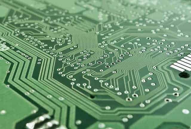
A printed circuit board or a PCB can provide mechanical support to electronically connected electronic parts of a device using traces etched using copper sheets, conductive pathways, etc., laminated on a non-conductive substrate. Usually, preset IPC organization standards help design the PCB layout, maintain a certain level of quality, and follow an excellent turnkey PCB assembly pattern accepted by the industry. PCBs usually follow the IPC 2221A standard in design and quality control, which is the same for any material the PCB is made with. An insulator is a prime component of any PCB, home to various layers of materials attached to the insulator itself. All these layers act as a form of grounding to the entire PCB. Now coming to the copper traces – they are created either by the mechanical laying of individual lines or by applying a copper coat to the entire board and stripping away what is left after your work is done. The second process is much more efficient, as this ensures that you have the exact amount of copper traces required on the PCB for connecting electronic components.


