
Probably everyone knows what logical IC’s and how to use them in the design are. But if the design is more complex, electronics enthusiasts are more likely to choose microcontrollers as they minimize the count of external components. But the problem is that not everything is possible with microcontrollers. They have many disadvantages when a fast response to input signals is needed. Microcontrollers execute operations one by one in sequence (conveyor). So output results will occur after some number of clock cycles. One way is to use hard logic IC’s. But when complexity grows – the number of IC packages also increases. This way design board becomes tremendous. So where programmable logic devices (PLD) comes to help. CPLD devices have many base elements (gates) without strict electrical interconnection. So designer can program these connections to combine any logical combination. Programmable logical devices allow the construction of any logical device, including counters, triggers, etc. The limit is only the number of base elements and connection lines.
So it is better to start with learning tools that allow the construction of logical circuits, simplify them, and avoid many mistakes. One of them is MAX+plus II BASELINE and CPLD from ALTERA. This software allows designing logical circuits visually that later can be flashed to a CPLD device. CPLD devices may be based on EPROM, EEPROM, and FLASH technology. I think FLASH technology is most attractive for radio hobbyists because it allows reprogramming multiple times without pain.
In this guide is the designing and programming process of Altera CPLD EPM3064A described. This device is quite cheap and affordable for most hobbyists. It has 44 pins on the PLCC package. Other features include the JTAG interface, ISP programmability, 1250 programmable gates. Core voltage is 3.3V, while I/O maybe 5; 3.3, and 2.5V. Maximum clock frequency 224.3MHz. It has buss friendly architecture with slew rate control, I/O can be configured as open-drain, power reduction to 50% mode; security bits for protection, and more. Device block diagram:

The MAX3064A architecture is based on the linking of high-performance Logic Array Block (LAB). Each LAB consists of 16 macrocell arrays. Each LAB is linked together via the PIA bus. Each Logical Array Block is fed by 36 signals from the PIA bus and control signals. More information about chip structure you can read in the datasheet.
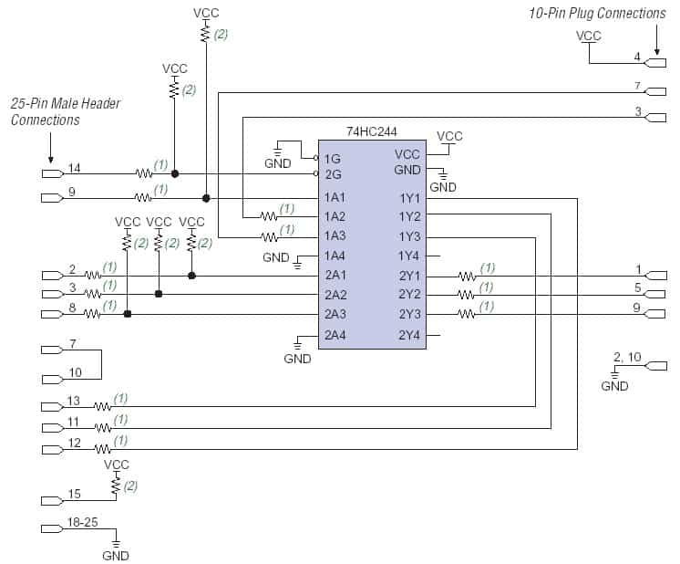
In order to program these devices, there is a special adapter used so-called ByteBlasterMV.

The adapter allows fast and effective programming of CPLD devices without significant investment. CPLD can be programmed In System. This means that you don’t have to remove the chip from the circuit when programming device pins enter the high impedance stage to protect themselves from unintentional conflicts with another board component.
The programming adapter is straightforward to build. And it can serve to program many other devices that support ISP, including microcontrollers.
Let’s move to design. As we mentioned, for a designing project, we will use MAX+PLUS II from Altera. So you can download it and install it. Then get a license for MAX+PLUS II Software for Students and Universities for version 10.2, 10.1, or 9.23 and press continue to get the registration number.
Then enter your hard disk number(You can obtain your hard drive volume serial number by typing dir /p at a DOS or command prompt on your PC ). Then press continues and fills the form. Then save generated license.dat file, which will be sent by email to your computer. Then install MAX+PLUS II and then setup the license by browsing to license.dat Under Options->License Setup menu. It shouldn’t be a problem.
MAX+PLUS II system has a convenient Graphical interface for project input, compilation, and flashing. The circuit may be described in AHDL, VHDL, Verilog HDL languages or construct circuits graphically. The project file may be graphical, text, or signal. The compiler may process the following project files:
- Graphical (.gdf);
- AHDL (.tdf);
- Signal (.wdf);
- VHDL (.vhd);
- Verilog (.v);
- OrCAD circuits (.sch);
- input files (.edf);
- Xilink Netlist (.xnf);
- Alptera project (.adf);
- digital automaton (.smf);
- other auxiliary files.
Let’s create a simple project. For this, create a working directory like C:\ALTERA_WORK\ this is where we will save our project files. The Pres File->New and choose Graphic Editor file and press OK. And save the project by naming schetchic.gdf and then select Set Project to Current File in the Project menu. The press Assign button and select Device EPM3064ALC44-4 from device family MAX3000A.

If you leave Auto in devices, then the compiler will select the device depending on project size.
In library you can find primitive components:
Logical primitives (located in c:\maxplus2\max2lib\prim\) like AND, OR, NOR with various number of pins;
Discrete logic analogs 74 series(located in c:\maxplus2\max2lib\mf\);
Parametric logical functions that allow the creation of any type and any complexity of logical devices (located in c:\maxplus2\max2lib\mega_lpm\).
Let’s create our own directory to store personal component library C:\ALTERA_WORK\Altera_Lib and connect this directory to the project in Options->User Libraries and enter the path to this directory (c:\altera_work\altera_lib ). You can enter symbols to the screen in two ways: by pressing the left mouse button in the work area and selecting Enter Symbol or selecting Enter Symbol from the Symbol menu bar. You can find drawing/editing buttons in the left bar so you can connect symbols with lines. Input and output pins can be selected from the element library named input and output(also, you can add names to each). If you need to see to 0 or 1, select VCC or GND. If you need to create your own symbol, then open a new graphical window, draw a component circuit, save it to c:\altera_work\altera_lib directory, and add this file to the project.

If there are no errors, you can test this circuit with the simulator. For this, open Waveform Editor and save the file with the same name. In the first row on Name, press the right mouse button and select the menu Enter nodes from SNF. In opened window pres List and then in the window, you can see all the circuit’s inputs and outputs. Select Both nodes and assign with =>. You can see waveform where you can set the value to 0 or 1 or set level change during time flow in the editor.

To simulate output select Simulator. It automatically generates output signal waveform:

If the model works OK, we can draw the model symbol by selecting the File->New->Symbol Editor file. Draw symbol and assign pin by double-clicking left mouse button and entering Full Pinstub name. Save the file with the same name as the model.
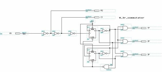
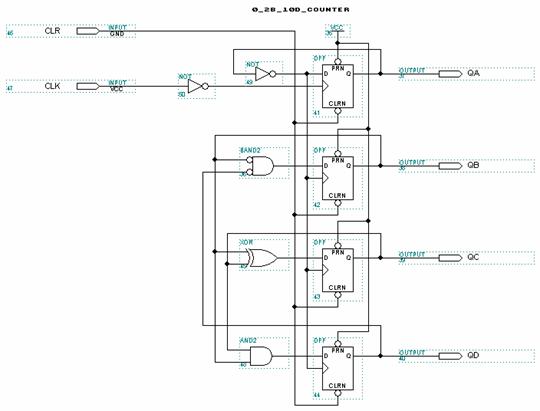
To give an idea, let’s go through a three-phase counter project with dynamical indication on three 7 segments LED displays.

 All components have to be created as described above. Main project looks like this:

0_3r_commutator is a three-phase commutator that dynamically switches each 7 segment LED indicator one by one and gives a control signal to multiplexers. Multiplexers connect decimal counters 0_2b_10d_counter depending on which indicator is ON. Decimal counters are connected to binary-seven segment decoder 0_bcd_7seg. So each component has to be created separately and saved in your library folder.
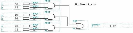
When models are saved in the library you can use them in the main project multiple times.
After all, the project is set, you can simulate the overall project with the simulator. An see all device working waveforms:

If the project seems to be working without errors, you can assign inputs and outputs to real IC pins. You can do this with FloorPlan Editor. And then compile the project. After this connect the ByteBlasterMV programmer to the device board and press the Program button in the Programmer window. And the project will be flashed.
As you can see MAX+PLUS II is a really good tool for creating complex logical functions in an easy way. Graphical editing saves tons of time comparing to writing in any HDL language.
Source: radio-konst.narod.ru
Dear Sirs:
I think so many people have the same problem that I have which is wanting to learn PLDs i.e.:PAL,GALs and CPLDs in a manner like learning microcontrollers way of learning ,I mean by that is first of all liting a L.E.D ,driving a 7segment and so on,so can you recommand me a way to do so ,please.
With very advanced thanks:
Abdullah Savas