When you are done with a clean period of task – designing, drawing a circuit, and tracing a PCB, you need to transfer a design to a real board. Here starts what I call a messy part of the design. When designing at home, there are several options – to use prototyping boards or make PCB by yourself. You have to transfer the PCB image to a board with a copper layer in the second option. There are several methods of doing this: direct transfer with glossy paper where the image is printed with a laser printer or more advanced ultraviolet exposure. This way, the PCB image is printed on paper or film directly from the program window without keeping in mind PCB file formats. A different situation is when fabricating professional PCB’s. Each company that fabricates PCB boards always announce what type of file formats they support. So if you are going to order a PCB, better check with them to save your time.
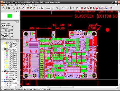
The most common and standard format is the so-called Gerber file format. Almost all layout tools can produce Gerber files. If you want to preview your generated Gerber files, there is a nice free Gerber file viewer(GCPrevue) from GraphiCode, Inc. (http:\\www.graphicode.com) to use.

Or you can use another Free Gerber Viewer – gerbv.
Same Gerber standard has many variations but here are two main:
- Standard Gerber – like RS-274-D, which requires an external aperture list to define all the apertures in the design;
- Extended Gerber – like RS-274-X, which contains all aperture definitions within a file.
Mostly there Extended Gerber is used.
PCB manufacturers have to transfer the image to PCB; They usually use a Photoplotter to expose the circuit board’s resist layer with the image. The resist layer controls the removal of copper during the etching phase. A photoplotter draws an image with light according to data in the Gerber file. Photoplotter contains a specially shaped aperture that controls a light passing through. Photo plotters can be raster or vector. Most of them are raster.
Other methods are exposing circuit board through very detailed transparent material or more time consuming is direct engraving.


Great article