
PCBs are the neatest and professional-looking among the assembled circuit types. But soldering is still required on the copper patterns on the board. In the early 1900s, before printed circuit boards existed, the only way circuits were made for electrical or electronic components was by wiring them point to point on a chassis. These chassis were either a pan or a sheet of a metal frame with a wooden bottom. The components attached to this chassis were connected with either wire connector lugs or crimp connectors or via jumper wires by soldering their ends or some other method. These primitive methods made circuits very fragile and large or bulky, and their production was very labor-intensive, so the products were expensive.
Albert Hanson, a German inventor, thought flat foil conductors joined with a board insulated in multiple layers in 1903. The very next year, in 1904, Thomas Edison was experimenting with chemical methods to plate conductors on paper. But it wasn’t before 1913 that the printing and etching method was patented; Arthur Berry in the UK coined this method. These printed circuits did not come into common consumer electronics until the 1950s.
PCBWAY Community
In today’s modern world, there are many forums or communities for electronics online, and one of the very famous ones for PCB is the PCBWAY. PCBWAY is a place that brings manufacturers and customers together. They have more than a decade of experience in the fields of fabrication and prototyping of PCBs. PCBWay have proved their focus to their customers’ needs in terms of cost-effectiveness, delivery, and quality. And this can be vouched by their outstanding customer reviews. Not only has this PCBWAY provided a platform for students and electronic hobbyists to display their projects to the community and get a sponsorship if their work is up to the standards. Check out the large pool of sponsored projects here.
Sponsorship
PCBWay has already sponsored newly 1700 projects of a total value of approximately $83000. Their strong belief in non-profit projects and education makes them stand out amongst other manufacturers. If you or your team is working on a new project where PCB is an essential part, you can apply to get sponsorship by sending a detailed description with pictures of what you are working on. Upload your PCB files, and soon enough, you may be getting coupons to finance your PCB manufacturing.
Crowdfunding
Besides direct sponsoring distinct projects, PCBWay also has a separate branch on sponsoring non-profit or educational projects. The aim is to encourage enthusiasts to accomplish their design ideas before they get lost. They are offering support for crowdfunding projects. The amount varies, but for instance, in 2018, they offered $50000. Also, they share cash coupons via social media. If you have launched or plan to start a crowdfunded project, send details to sponsor@pcbway.com. After approval, you will get the corresponding cash voucher or discount voucher into your PCBWay account for the PCB prototyping run or production run.
What is the PCB manufacturing process?
PCB manufacturing from the point of design to an actual circuit requires many steps in between; here is a summary of those steps. You can check out more detailed manufacturing steps and capabilities at PCBWay.
Design and Output
In essence, a circuit board has to be compatible with the designed layout of the PCB. A few commonly used design software for PCB are an eagle, Pads, OrCAD, Altium Designer, and KiCad. After the design is finalized, it is exported to production. Usually, the production of PCBs is done by software called Gerber or IX274X.
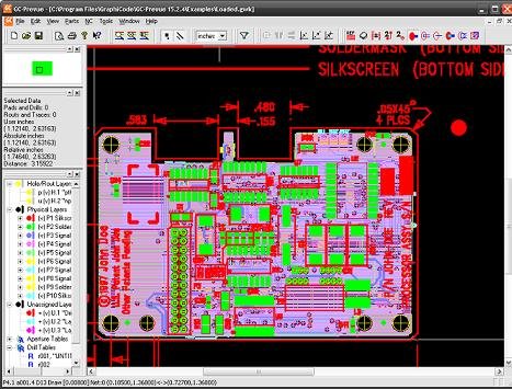
The Gerber file of the PCB design consists of comprehensive information like component notation, apertures, copper tracking layers, drill drawing, and other options. One of the exciting features of this stage is that the PCB design goes through a troubleshooting process by the software so that no errors are left unanswered. The designers can even alter things like board edge spacing, hole spacing, hole size, trace, and track width. After everything is done and dusted, the PCB file is forwarded to the PC board houses for production.
From File to Film
So the next step is the PCB printing which is done after the PCB design is finalized and sent to the manufacturers. The manufacturers will, in turn, perform their own DFM check before moving towards the actual printing. This printing is done by a special printer called the plotter, an exact laser printer that makes photo films of the PCBs to print the circuit boards. The printer’s output is a photo negative of the PCB in black ink, where for the inner layers, black ink represents the conductive copper part, and the clear portion represents the non-conductive part. For the outer layer, this representation is reversed. The clear part is the copper, and the black ink is the non-conductive part.
Printing the inner layer
Till the last step, only films were made to map out the copper paths. A basic PCB only comprises the laminate board whose core material is a glass fiber and epoxy resin. The board is ideal for receiving copper, and the epoxy resin provides a dust-resistant and sturdy start point for the PCB. It is part of the process to whittle away the copper to reveal the paths made in the design. While doing this, keeping the panel clean as a single speck of dust may result in shorting the circuit. In the end, the panel is covered with a photo-sensitive film which hardens on exposure to UV light. Both the photosensitive film and Photo film are blasted with light, and the clear parts remain unaffected while the paths harden and the film fits into the pins that hold it over the laminate panel.
Cleaning the unwanted copper
So now we have a PCB with the copper paths covered in the hardened film. The next step is to remove the excess copper, which is done by a chemical called the copper solvent solution bath. This solution will remove all the copper that is not covered by the hardened film. After the excess copper is removed, we now must remove the hardened resist. Another alkaline solvent does this, and after completion, the board will only have the copper in the PCB design. This process is referred to as etching.
Layer up and bond
This a 2 step stage; now, the individual PCB layers are to be combined to give the circuit board a proper shape. The two steps are
- bonding
- layer up
The bonding is done in a table of steel with metal clamps. The layers fit into the pins attached to the table, which causes the layers to fit perfectly and avoid shifting during alignment.
The outermost layer is made from pre-impregnated epoxy resin and sheets of fiberglass. There is also a thin copper foil that covers the bottom and top of the substrate. A technician will start to place this thin layer on an alignment basin. After this, a copper press plate and aluminum foil will be used to complete the stack of layers.
After this, the stack undergoes computer bonding presses where it is heating to put pressure on the stack and then cool at a steady rate. Now all the technician needs to do is remove the PCB from the pins where it was holstered, and we would have a multi-layered PCB freshly made.
PCB Drilling
To attach components to the multi-layered PCB, we use VIAS drilling. The drill makes holes in the shape of annular rings that are pated-through. A Dremel drill press with drill bits made out of tungsten carbide is commonly used for drilling. The bits are normally 0.035 inches, and in case of high volume, automated drills are used. For tiny holes, laser drills VIAS provides an interior surface finish inside the holes.
Conductor Plating
So the outermost layer of the PCB is not solderable as it contains copper connections where the components are attached. To make them viable for soldering, the surface is plated with some other conductor; usually, nickel, tin, or gold is used to make the PCB solderable again.
Solder resist
Just like initially, we covered the copper that was included in the design again. We would use solder resist for the parts which are not to be soldered. The polymer coating is also essential to ensure that nearby component leads or copper paths don’t get shorted out by solder traces.
Silk Screen
The almost done PCB board is sprayed with inkjet writing on its surface, displaying all the necessary information needed by the customer. After which, the PCB is sent to the curing and coating stage.
PCB Testing
After everything that was mentioned before this part, now comes the time to test our PCB. For example, many can be done, such as CT scanning test, Rigid Needle adaptor, and bed of nails test. But the basic and most commonly used one is when a computer program is used to drive small voltages at certain key points of the PCB and check that the applied voltage comes upon corresponding points similar to an electrical troubleshooting method.
PCB assembling
This is the final step before we can call our PCB an end product, and in this step, we are to assemble all the electronic components on their respective positions marked by the holes we drilled earlier. Two methods achieve this
- Surface mount construction
- Through-hole construction
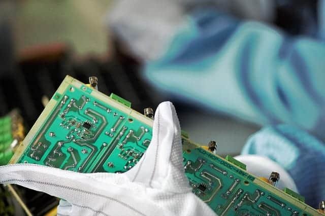
In the surface, mount construction method, a pad with legs similar to that of the PCB design is inserted, and the ICs are fixed in them. While in the through-hole construction method, the components legs are inserted in the holes that we drilled previously. In both methods, the component is mechanically and electrically fixed to the board with the help of a molten metal solder, and finally, the PCB is complete and ready for use. PCBWay is always offering a great PCB assembly price and a quick turnaround.