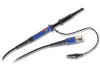
Testing pulse transformer with an oscilloscope
Pulse transformers are a little different from regular AC transformers. In AC transformers, magnetic flux alternates between negative and positive values in the core, while in pulse transformers, magnetic flux is unipolar. Pulse transformers are used in TV, computer power supplies. If you need to test a pulse transformer, it may be almost impossible to do this with an ohmmeter, even a digital one, because the windings of impulse transformers have meager active resistance except for high voltage ones. One way to test is to measure the inductance of windings and compare them to values in specifications. Still, not everyone has the ability to measure inductance, and not always you have transformed specifications near by. So there is another way to test pulse transformers, which may be acceptable to almost everyone radio-hobbyist, using a low-frequency generator that works at the resonance frequency of contour, which consists of external capacitor and pulse transformer winding.