In electronic circuit drawings, there are two types of objects: component symbols and nets. Nets represent wires connecting the components – which represent physical devices. In the example below, we see component type MAX3232. U2 is a reference label of a component. Electronic component usually has pins. Pins always have their numbers starting from 1. Pins also have their names. They are usually written inside component blocks like C1+.

For this particular component, we used the U2 label. U (or IC) label applies to all semiconductors. But you know that resistors usually are labeled as R1, R3. Capacitors C1, C2, Diodes – D1, D2, Transistors Q1, Q2, Crystals – X1, X2, X3, Jumpers J1, J2, J3, Inductors L1, L2.
Other semiconductors devices may have special labels like RAM0, RAM1.

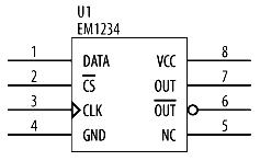
Let’s go further and talk about PIN characteristics. In figure 2 we can see:
- Pin 1 – is a generic pin;
- Pin 2 has a bar over the name. This means that activity is low signal;
- Pin 3 indicates that this is edge-triggered input. Input responds on signal level change;
- Pin 4 and Pin 8 are GND and VCC (VDD). VCC stands for ‘collector’ on the other hand, VDD stands for ‘drain.’ This is just terminology. Both of them mean voltages.
- Pin 7 is output-active high;
- Pin 6 is output active low;
- Pin 5 is labeled as NC – this means Not Connected.
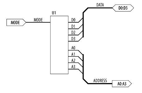
Related signals may be routed using a bus wire.

In figure 3, there is a generic subcircuit, which can be used in many designs. You see that there are Ports used that indicates the direction of signals. D0:D3 port is bidirectional, port A0:A3 is an output, and port MODE is as input.

In figure 4, there is shown how correctly wires should be drawn. If wires are interconnected, then a dot should be drawn. Otherwise, wires are just crossed, which means they are not connected.

Always use ground symbols down and power source up.


thanks
Jamin