Soldering is finished next step is to run fast tests on the AVR DDS signal generator to make sure everything works as expected. It appears that rush design has its consequences, but with few tweaks, it works.

First of all, errors found on board.:
- In zeroing offset voltage circuit resistor R5 value was left 100k – should be 33.33k;
- In filter circuit C2 was 33pF should be 18p;
- Filter switch connected wrong – it should not short filter but disconnect its output when not used;
- Filter op-amp pins 6 and 7 were left unconnected. Solder bridge fixes this;
- RESET2 line needs a pull-up resistor. Alternatively, the internal pull-up can be enabled in Atmega328 PB1 pin;
- RESET1 line needs series 0.1uF cap to work with Arduino bootloader;
- Resistors footprints are too small (4mm) could be 6.3mm to fit the ones I have;
- Bad PCB ground pouring results in parasitic op-amp capacitance. It results in signal ringing and overshooting. Partially can be fixed with the feedback capacitor. But needs a new PCB where the ground plane is removed around trace to inverting input.
Running simple code
To test both microcontrollers and the analog part, I wrote a couple of simple programs for each MCU. First displays demo text on LCD to make sure it works. More info on programming LCD is here. The more exciting part is the signal generation and an analog circuit. I used signal tables stored in the internal microcontroller er FLASH to output the test signal and sent samples to the port using the pgm_read_byte() function in an endless loop. Here is a fragment of code:
const uint8_t squarewave[] PROGMEM= //square wave
{
0x00,0x00,0x00,0x00,0x00,0x00,0x00,0x00,0x00,0x00,0x00,0x00,0x00,0x00,0x00,0x00,
0x00,0x00,0x00,0x00,0x00,0x00,0x00,0x00,0x00,0x00,0x00,0x00,0x00,0x00,0x00,0x00,
0x00,0x00,0x00,0x00,0x00,0x00,0x00,0x00,0x00,0x00,0x00,0x00,0x00,0x00,0x00,0x00,
0x00,0x00,0x00,0x00,0x00,0x00,0x00,0x00,0x00,0x00,0x00,0x00,0x00,0x00,0x00,0x00,
0x00,0x00,0x00,0x00,0x00,0x00,0x00,0x00,0x00,0x00,0x00,0x00,0x00,0x00,0x00,0x00,
0x00,0x00,0x00,0x00,0x00,0x00,0x00,0x00,0x00,0x00,0x00,0x00,0x00,0x00,0x00,0x00,
0x00,0x00,0x00,0x00,0x00,0x00,0x00,0x00,0x00,0x00,0x00,0x00,0x00,0x00,0x00,0x00,
0x00,0x00,0x00,0x00,0x00,0x00,0x00,0x00,0x00,0x00,0x00,0x00,0x00,0x00,0x00,0x00,
0xff,0xff,0xff,0xff,0xff,0xff,0xff,0xff,0xff,0xff,0xff,0xff,0xff,0xff,0xff,0xff,
0xff,0xff,0xff,0xff,0xff,0xff,0xff,0xff,0xff,0xff,0xff,0xff,0xff,0xff,0xff,0xff,
0xff,0xff,0xff,0xff,0xff,0xff,0xff,0xff,0xff,0xff,0xff,0xff,0xff,0xff,0xff,0xff,
0xff,0xff,0xff,0xff,0xff,0xff,0xff,0xff,0xff,0xff,0xff,0xff,0xff,0xff,0xff,0xff,
0xff,0xff,0xff,0xff,0xff,0xff,0xff,0xff,0xff,0xff,0xff,0xff,0xff,0xff,0xff,0xff,
0xff,0xff,0xff,0xff,0xff,0xff,0xff,0xff,0xff,0xff,0xff,0xff,0xff,0xff,0xff,0xff,
0xff,0xff,0xff,0xff,0xff,0xff,0xff,0xff,0xff,0xff,0xff,0xff,0xff,0xff,0xff,0xff,
0xff,0xff,0xff,0xff,0xff,0xff,0xff,0xff,0xff,0xff,0xff,0xff,0xff,0xff,0xff,0xff,
};
void signalOUT(const uint8_t *signal)
{
	uint8_t i;
	i=0;
	do
	{
		PORTD=pgm_read_byte(&signal[i++]);
	}while(1);
}
int main(void)
{
	PORTD=0x00;//set initial zero values
	DDRD=0xFF;//set D port as output
    while(1)
    {
		signalOUT(sawtoothwave);
    }
}
Let us see how it appears on an oscilloscope. First of all, let’s see how sinewave performs.

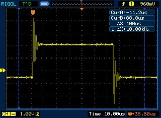
The sine wave seems to be OK as it doesn’t have fast-rising edges. The different talk begins when generating a square wave:


Here things look bad. Due parasitic capacitance on negative feedback input of operational amplifier signal overshoots and rings. Let us try to pass this signal through the filter:

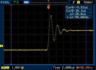
The filter removes overshooting and ringing but also distorts the signal itself by integrating it – not the best solution. PCBs are already made – we cannot remove the ground plane. We can still try to compensate for parasitic capacitance by adding a small capacitor in parallel with the feedback resistor.

Added 6.8pF cap and things started looking better:

It didn’t have a slightly bigger cap like 10pF – it would remove what’s left of ringing. For now, I’m going to leave 6.8pF here. I hope better PCB tracing will eliminate this problem.
Triangle signal looks good as there is no sudden signal level change:

The sawtooth signal has the same problem as the square – on sharp edges there is a ringing left.

Speaking of Signal offset and amplitude control – it works like a charm as modeled here. There aren’t noticeable distortions in all control range as there were on AVR DDS V2.0.
If you have any other thoughts about removing signal ringing or have suggestions on better PCB tracing and ground planes, please leave a comment. Download avrdds3_3 files with fixes made so far. Here is also a program test files for running LCD on Atmega328P and generating signals on Atmega88.


Is look up table is need for square generation, without the look up table we can generation all waveform except the sine wave. sine wave needs look up table. which oscilloscope do you use?
Yes, I have thought about this. We do not need table to output values. May this can improve speed of frequency generated?
Instead of using a table to generate the signals, perhaps an algorithm could generate signals even sine.
Thanks guys for ideas. It sounds logical to generate square waves without using DDS. but for sinewaves for and other shape signals it becomes harder and might reduces max frequency even further. Did you see that DDS algorithm uses 9 MCU clock cycles for a single sample? There are 256 samples in one signal period. So it is easy to calculate max signal frequency without loss of resolution. Would it be possible to make in less cycles and still have control of frequency? For higher frequencies it is best to use specialized DDS chips.
Thanks Alex and admin for your reply, 256 samples in one signal period is much better sampling rate, but 9 MCU cycles for single sample means the DDS algorithm taking more MCU time when the number of cycles increases.
Can you give me the range of frequencies that DDS algorithm works better without any loss of precision.
Hi, how can I order PCB for this project, and is there any progress in the work?