
You have taken weeks to design your PCB and carefully routed traces and placed components and reread your schematic. And here comes the moment of truth, sending your design over to fabrication. However, one more step, which needs to be taken before you press that submit button, is checking your Gerber files, as this will save you a lot of money spent on making expensive errors and losing time on long waits.
The language used between PCB designers and PCB manufacturers is Gerber files, which is universal. They have everything in it to make your board: from copper tracks to holes to make. Consider these as the design of your PCB and like any other design, it must be precise and comprehensive. We shall take a stroll of what you need to verify before transferring these crucial files to your manufacturer.
Getting to Know What Gerber Files Are
It is always useful to know what you are working with before going down to the checklist. A set of standalone files, each corresponds to one of the layers or aspects of your PCB, is referred to as Gerber files. You will normally have top and bottom copper, solder mask, silkscreen, paste mask for SMT assembly and drill files indicating the locations and sizes of holes.
Today modern designs tend to use the extended Gerber format (RS-274X or Gerber X2) differing in that it puts extra information into the files. This renders them more trustworthy and eliminates the possibility of misunderstanding by the manufacturer.
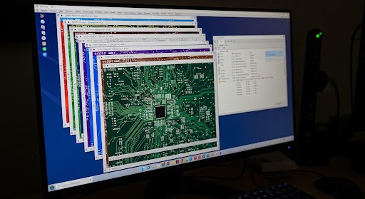
Ensuring Layer Alignment and Registration
Misaligned layers are one of the most frequent problems that can be a setback in your PCB project. Your Gerber files have to be perfectly aligned across each other, or you will wind up with vias which are not meant to connect, pads which do not fit into their holes, or traces which short together inappropriately.
The most efficient approach to detect these issues early is to open an online gerber viewer in which one can overlay the different layers and switch them on or off. Place all of your files and ensure a logical check that the pads match the holes of the drills, that the holes of the solder mask match the copper pads underneath them, and that multilayer boards are properly aligned by the via holes using all layers.
Note any mechanical characteristics such as mounting holes or board cut-outs. These must comply with your copper characteristics, particularly when you are creating something such as a Flex PCB Manufacturer would create, in which mechanical stress points are even more important than on rigid boards.
Inspecting Trace Widths and Clearances
Most spacing violations were likely to be detected by your design rules checker in your CAD software, but it is still worth making a visual inspection of your Gerber files. Find regions where traces intersect each other particularly in dense areas around the fine-pitch components.
Ensure that the minimum trace widths that you have are within the capability of your manufacturer and your requirements. In case you are connecting a large current through some traces, check their size with such tools as Free Wire Gauge Calculator and make sure that they would not be overheated in the process.
Obvious clearances between copper features and board edges should not be overlooked either. The majority of manufacturers will insist on some kind of keepout area surrounding the board perimeter and going against this may result in manufacturing errors or even just rejection of your design.
Examining Drill Files and Hole Sizes

Drill files are used to specify the locations of each hole in a board, starting with the tiny vias and ending with the big mounting holes. Begin with the checking that your drill file format is how your manufacturer expects it to be—usually Excellon format, but that could vary.
Ensure that the holes that are being drilled are in the right positions and none are missing. Add up your special hole sizes–a variety of dozens of different drill sizes can add to the manufacturing time and cost. In case, reduce to a smaller range of sizes, which will still satisfy your design needs.
In the case of plated through-holes, the annular ring (the copper pad surrounding the hole) is to be sufficient. Smaller, and the drill may pierce right through the pad. Most manufactures give a minimum annular ring size, which is usually in the range of 4-6 mils in the case of standard production.
Reviewing Silkscreen and Reference Designators
The outlines of your components, reference designators, logos and other text in your board are contained in your silkscreen layer. Silkscreen errors are not critical to functionality but assembly and debugging can be annoying.
Check all reference designators and ensure that they are readable, properly positioned and do not encroach on pads or vias where they would be covered with solder mask or components. Ensure that your text size is not less than the minimum of the manufacturer, which is usually about 40-50 mils to make sure it is reproduced reliably.
Assuming that you have added diode, capacitor, or connector polarity markers, make sure that they are correct. Your main documentation in this physical board is silkscreen and any mistakes during this step may result in some errors in assembly.
Validating Solder Mask and Paste Mask Layers
Solder mask covers your copper in case of oxidation and it stops the formation of solder bridges in the assembly process. Ensure that your solder mask holes are sufficiently transparent to expose all pads which require soldering and are not covering up all other. Specific attention should be given to fine-pitch components in which a lack of solder mask between pads may result in bridging.
In SMT-component manufacturing, your solder paste mask layer will define where the paste gets deposited. These apertures are often a bit less than the pad dimensions below to avoid a little surplus paste that could otherwise form bridges.
Running Final Cost and Capability Checks
It is wise to ensure that you check whether your design is within your budgets before getting yourself committed to fabrication. There are numerous PCB Cost Calculator available with many manufacturers that take into account the factors such as board size, the number of layers, the type of material and the quantity. Conducting this check will allow you to know whether any design decisions are needlessly increasing the costs.
Likewise, ensure that your design is within the capabilities of your manufacturer. Things like minimum hole size, trace width, and layer count always affect manufacturability and price.
Your Turn to Act
A thoroughly checkup on Gerber files preceding fabrication is not only about defect-avoidance, it is a solid assurance that what you thought you got is what actually comes back in the boards. Invest the hard work now, and it will save you later from receiving a stack of boards whose functionalities are shorted a mile from satisfaction.