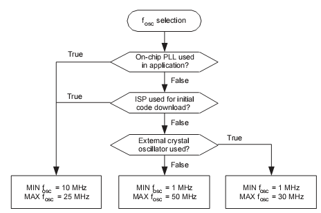
ARM microcontrollers can be clocked in several different ways. One way is to use an external clock with a duty cycle of 50-50 and a frequency range from 1MHz to 50MHz (LPC21xx series) connected to the XTAL1 pin. Another way is to connect the External crystal oscillator, but its range is lower (1MHz to 30MHz for the LPC21xx series). And last but not least is the on-chip PLL oscillator, then external clock source frequency should not exceed range from 10MHz to 25MHz. Let’s analyze more deeply each clocking mechanism.
In the picture above there is fosc selection diagram shown.
External clock source
This mode is also called slave mode because the master clocking circuit does its clocking – ARM doesn’t act as a clock generator. This mode clock source is connected to ARM through the XTAL1 pin and should be coupled with a capacitor of 100pF. The amplitude of the clock signal should be at least 200mVRMS. XTAL2 pin can be left unconnected in this case.:
Signal frequency can be in the range from 1MHz to 50MHz with duty cycle 50 – 50.
Oscillation mode: External crystal only
In this mode, ARM clocks itself with the internal circuit. Just external crystals and capacitors are needed. Using this oscillation mode, the crystal clock frequency can be chosen in the range between 1MHz and 30MHz (LPC21xx series):
For capacitor values refer to datasheet.
Oscillation mode: External crystal with PLL
PLL (Phase Locked Loop) is used to generate a system clock from between 10MHz to 25MHz. PLL may multiply frequency to range from 10MHz to 60MHz (LPC21xx series) and 48MHz for USB if used. PLL uses a frequency multiplier, ranging from 1 to 32 (practically, this value cannot be higher than 6 due to the upper-frequency limit).
PLL generator allows running ARM at high speed with low-speed oscillator connected. Also, this minimizes EMC emission as the frequency is multiplied inside the ARM chip. PLL also allows changing frequency dynamically. It may raise calculation power when it is needed and lower frequency when power saving is needed.
PLL unit itself uses CCO(Current Controlled Oscillator), which operates in the range of 156MHz to 320MHz, so there is an additional divider that keeps CCO within its range, while PLL provides the desired frequency. The output clock is generated by dividing CCO frequency by 2, 4, 8, or 16. The minimum divider is 2, so the output of PLL will always have a duty cycle of 50% for sure.
PLL Activation and control are done via the PLLCON register. Register PLLCFG controls PLL multiplier and divider values. These registers are protected from the accidental alteration of PLL parameters or deactivation of PLL. Let’s see how this is done in practice.
Say we have a 12MHz crystal connected to LPC2148. Then we can say Osc=12MHz. We want core frequency to be 60MHz, then we have to multiply crystal frequency by five:
Cclk = M * Osc = 5 * 12 = 60MHz;
The second thing is that we have to keep OCC oscillator frequency (Fcco)within its range [156Mhz-320MHz], so we have to control another constant P:
Fcco = Cclk * 2 *P;
Fcco = 60MHz * 2 * 2 = 240MHz;
So we can have P=2 ant this meets CCO requirements
(156MHz < 240MHz < 320MHz).
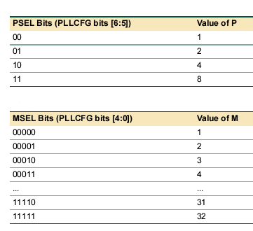
Programming PLL has to be done in some sequence to make new PLL settings effective. First of all, we have to write Multiplier M and divider P values to the PLLCFG register. Since M and P values can have only specific values, then there is a lookup table used to determine PLLCFG bits:
So for our calculations M=5 and P=2, then PLLCFG=0b00100100=0x24;
Further, there has to be some sequence of activating PLL. After the PLLCFG register is updated, update the PLLCON register, and then you have to write 0x000000AA and then 0x00000055 to the PLLFEDD register. These values have to be written on consecutive cycles.
For instance using C PLL initialisation would look like:
void PLL_Init(void)
{
PLLCFG=0x24; //Multipler and divider setup
PLLCON=0x01; //Enable PLL
PLLFEED=0xAA; //Feed sequence
PLLFEED=0x55;
while(!(PLLSTAT & 0x0400)) ; //is locked?
PLLCON=0x03; //Connect PLL after PLL is locked
PLLFEED=0xAA; //Feed sequence
PLLFEED=0x55;
VPBDIV=0x2; //peripheral bus runs 2 times slower
}
Note that power-down mode disconnects and turns off PLL. Waking up doesn’t restore PLL – you have to do this in software. You can call the PLL activation routine at the beginning of any interrupt service routine, which is called due to wakeup.


how to increase the frequency of out put of GPIO ?
Thanks for the share…………………really helped me….
Dear ALL,
I am using lpc2148 device in my circuit. But I am unbale to connect through JTAG. On the very first step it shows JTAG communication failure.
I am providing below the key poitns of the circuit.
1. I am using a 24 MHZ crystal oscillator, with o/p of the crystal oscillator directly connected to the device at XTAL1 pin.
2. XTAL2 pin is left open.
3. Voltage on connect pin (Pin no 17 of LPC2148) is 2.2 V, Whereas the power in voltage is 3.3 V.
4. Reset Pin(Pin no 57 of LPC2148) is High.
Please suggest whether the crystal oscillator or any other thing may be troubling the operation.
TIA
Pras
why is the code snippet above for PLL is not working in keiluvision4 it says
ADC.c(133): error: #20: identifier “PLLCFG” is undefined
ADC.c(134): error: #20: identifier “PLLCON” is undefined
same for all PLL registers
why always the pll feed sequence in lpc2148 is 0xaa and 0x55. why is it so. what is the register format of pllfeed register. can we take the feed sequence other than this data